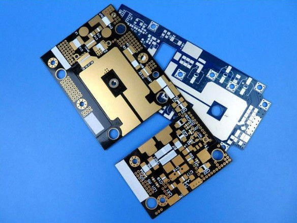
Designing printed circuit boards (PCBs) for radio frequency (RF) and microwave applications involves a unique set of challenges. These high-frequency boards require specialized layout, material selection, and manufacturing techniques to ensure signal integrity, minimal interference, and optimal performance.
This RF and microwave PCB design guide outlines key considerations for engineers and designers, while also providing practical tips for sourcing low to medium-volume PCB fabrication—ideal for prototypes, testing, and small-batch production.
What Are RF and Microwave PCBs?
RF PCBs are designed to carry signals typically between 100 MHz and 3 GHz, while microwave PCBs handle even higher frequencies up to 30 GHz or more. These boards are commonly used in:
- Wireless communication systems
- Radar equipment
- Satellite electronics
- GPS modules
- IoT devices
- Military and aerospace applications
Because of the high frequencies involved, even minor layout or material flaws can drastically impact signal transmission, leading to power loss, signal reflection, and electromagnetic interference.
1. Material Selection for RF/Microwave PCBs
Choosing the right substrate is the first critical step in RF PCB design.
Key material properties to consider:
- Dielectric constant (Dk): Stability is more important than low values. Variations in Dk can cause impedance mismatch and signal delay.
- Dissipation factor (Df): A lower Df results in less signal loss.
- Thermal stability: Materials should perform consistently across a wide temperature range.
Popular materials for RF/microwave PCBs:
- Rogers RO4000 series
- Taconic RF laminates
- Isola materials
- Teflon/PTFE composites (used in high-frequency military and aerospace applications)
These materials may be more expensive than standard FR4 but are essential for high-frequency performance.
2. PCB Stack-Up and Layer Management
Proper PCB stack-up design ensures controlled impedance and minimal crosstalk. RF and microwave PCBs often use a mix of RF, digital, and power layers, separated by ground planes for isolation.
Best practices:
- Use dedicated ground planes below RF signal layers.
- Avoid overlapping high-speed and low-speed signals.
- Maintain tight coupling between signal and ground layers to reduce EMI.
The layer count often depends on the complexity of the application, and many RF PCBs are built as 4-layer or 6-layer boards to balance performance and cost.
3. Controlled Impedance Routing
For RF signals, controlled impedance is crucial to ensure signal integrity. This involves maintaining consistent trace width and spacing based on the PCB’s dielectric properties and stack-up.
Guidelines:
- Use microstrip or stripline configurations depending on layer position.
- Maintain consistent trace width across the entire signal path.
- Use impedance calculators or simulation software to fine-tune routing.
Even small inconsistencies in routing can cause reflections, insertion loss, or degraded performance.
4. Minimize Discontinuities and Crosstalk
In high-frequency PCBs, physical discontinuities—like 90° trace bends, via stubs, or inconsistent trace lengths—can cause signal degradation.
To minimize these:
- Avoid sharp corners; use 45° bends or curved traces.
- Match trace lengths in differential pairs.
- Space RF traces away from digital traces to reduce crosstalk.
Additionally, blind and buried vias may be preferred in high-density designs to reduce unwanted parasitic effects.
5. Shielding and Isolation
RF circuits are sensitive to electromagnetic interference from nearby components or traces. Shielding and isolation techniques are used to reduce this:
- Use fencing vias (via stitching) around sensitive areas.
- Incorporate EMI shields for exposed high-frequency components.
- Separate analog, digital, and RF sections with clear ground boundaries.
Ground pours and copper islands can help, but they must be connected properly to avoid creating resonant cavities.
6. Low to Medium-Volume PCB Fabrication: What to Look For
Many RF applications—such as prototypes, early-stage products, or niche devices—don’t require high-volume production. Choosing a manufacturer that supports low to medium-volume PCB fabrication can help manage costs, reduce waste, and allow for faster iteration.
Key qualities in a fabrication partner:
- Experience with high-frequency materials like Rogers, Taconic, and PTFE.
- Controlled impedance manufacturing with tight tolerances.
- Quick-turn capabilities for small batches and prototypes.
- Design-for-manufacturing (DFM) support to catch issues early.
Look for a PCB fabricator that specializes in RF and microwave technologies and is equipped to handle hybrid builds with different materials or layer combinations.
Bonus Tips for RF PCB Success
- Simulate before fabrication: Use tools like Ansys HFSS or Keysight ADS to model signal paths.
- Include test points: Place accessible points for signal measurement and tuning.
- Work closely with your manufacturer: Share detailed specs, stack-up diagrams, and impedance targets.
A good manufacturer can offer layout feedback and help optimize your design for real-world performance and manufacturability.
Final Thoughts
Designing PCBs for high-frequency applications demands precision, planning, and deep understanding of RF behavior. By following this RF and microwave PCB design guide, you can reduce signal loss, minimize EMI, and create a reliable board for your application.
Whether you’re building a 5G antenna module, radar controller, or GPS transceiver, choosing a manufacturer that supports low to medium-volume PCB fabrication ensures you get the performance you need—without the cost or complexity of mass production.
Partner with a specialist who understands both the technical and manufacturing sides of RF PCBs. That way, your prototypes and production boards perform just as intended, every time.

